

Condensed Matter Physics Seminar Schedule
Condensed Matter Theory Faculty and Research
Center for Electronic & Magnetic Nanoscale Composite Multifunctional Materials (ENCOMM)
|
|
|
Links:
Condensed Matter Physics Seminar Schedule Condensed Matter Theory Faculty and Research Center for Electronic & Magnetic Nanoscale Composite Multifunctional Materials (ENCOMM) |
|
|
|
|
|
|
| Nonlinear dynamics, spatio-temporal chaos, and pattern formation in hydrodynamic flows; instabilities; convection in multilayer systems; viscoelastic flows and instabilities. |
|
Semiconductors; surface science; electronic materials interfaces; semiconductor growth, processing, and characterization; defects; laser annealing; luminescence; metal-semiconductor contacts; heterojunctions; nanoelectronics; optoelectronics. |
|
|
Superfluidity in 3He and 4He; ideal surfaces and interfaces in liquid and solid helium; spin waves; scattering of atoms and excitations at the helium surface. |

|
Conductive and semi-conducting state of electronic polymers; molecular and polymeric magnets; new polymers and polymer processing. |
|
|
Properties of electronic materials at low temperatures and high-magnetic fields; two-dimensional electron gases and Quantum Hall effects; electron interactions and correlation effects; disordered conductors, magnetic properties. |
|
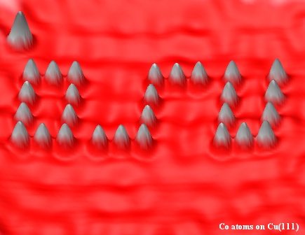
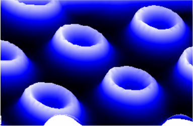
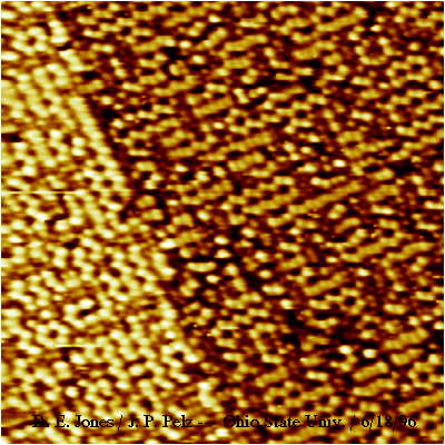
Using low temperature, ultrahigh vacuum scanning tunneling microscopes (STMs),we study the interactions of atoms and molecules on metal and semiconductor surfaces. The strength of such interactions can be controlled in structures that are built with atomic precision. Combining the STM with optical techniques (Raman scattering and ultrafast lasers) extends the range of vibrational and magnetic interactions that can be studied. The emergence of bulk properties such as magnetism, band structure and superconductivity in nanoscopic systems can be studied using this "bottom-up" approach. |
|
We study the electronic, magnetic and superconducting properties of materials ranging from multicomponent nanomagnetic materials and novel spin-electronic systems to ferromagnetic semiconductors using ultrahigh sensitivity Magnetic Resonance Force Microscopy—a scanned probe magnetic resonance imaging technique that employs mechanical detection to achieve exceptional detection sensitivity and spatial resolution. |
|
Control of the structure and composition of matter at nanoscopic length scales has
emerged as a grand challenge facing the scientific community. Specifically, one
area showing significant promise is the intersection of the emerging field of spintronics
with the development of nano-patterned materials. This promise arises from both
fundamental principles, such as the increased relevance of spin as an additional
quantum number in very small systems, as well as practical concerns, such as the
potential for significantly decreased power consumption and increased switching
speeds when spin currents are substituted for charge currents. Within this context,
our group focuses on three distinct but complementary approaches to integrating
spintronic functionality into nanoscale systems.
|
|
Magnetic and electronic properties of high temperature superconductors: two-coil penetration depth measurements; vortex dynamics and pinning; infrared reflectance measurements; thin film growth by coevaporation and sputtering; related single crystal growth. |
|
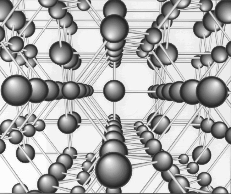
Structure and electronic properties of surfaces and interfaces: surface and interface science; atomic scale investigation/characterization of surface reactions; electronic transport phenomena at microscopic level. |

|
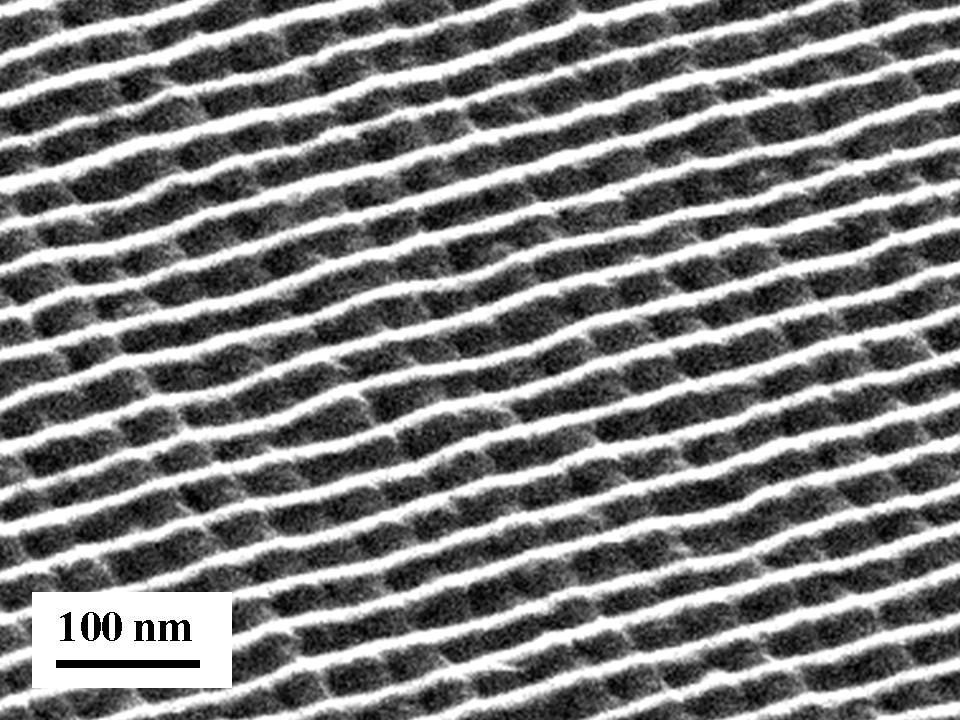
Optical properties of quantum well superlattices and two dimensional electron gas; surface acoustic phonons and elastic waves in lower dimensional systems; inelastic light scattering; Raman and Brillouin spectroscopy; optical properties under high pressure. |
|
|
Nonlinear response in ferromagnetic garnet thin films; magnetic, electrical, and optical properties of magnetic garnets; surface effects and long-range exchange coupling in magnetic/nonmagnetic metal layers and superlattices. |
 |
Spin transport behavior, such as spin injection, spin diffusion, and spin detection, in micro- and nano-structures consisting of metals, semimetals, and semiconductors; spin interaction and magnetic behavior in complex spin systems, such as spin density wave and rare-earth materials; transport properties of nanometer-size specimen using point contacts, nano-lithography and break junctions; growth of epitaxial layers by sputtering and e-beam evaporation in UHV. |
|
|
|
|
Nanoelectronic devices; Si-based tunneling junctions; polymer-based photonics and electronics; optoelectronic devices and integrated circuits; and semiconductor materials, fabrication and growth. |
|
|
Dr. Heremans' research is focused on the transport properties of nanostructures, particularly thermal transport. The emphasis lies on nanometer-scale structures suitable for energy conversion applications. He has three main subject areas: nanometer-scale scale thermoelectric materials; transport in carbon nanotubes, nano-composites and nano-fluids based on them; and nanometer-scaled wide-gap semiconductor particles (CuAlO2, WO3) that are potentially suitable for dissociating water photocatalytically. Dr. Heremans is an Ohio Eminent Scholar; Professor of Mechanical Engineering and Physics. |
|
Electronic materials; heterogeneous integration of dissimilar materials; optoelectronics, photovoltaics, molecular beam epitaxy, compound semiconductors, nanostructures, defect and interfaces, wide and narrow gap semiconductors. |
Mail questions and comments to Kris Dunlap .